darkspr1te
New Around Here
The reason for this post is so I can cover how I am recovering a asus rt-AC5300 back from the dead, or hope too.
In this thread i will be covering NAND reading, ecc systems, CFE's , bootloaders in general , JTAG , software source code & compiling.
It wont be a easy read to do guide as it's a project in motion and I may incorrectly cover items initially.
So the short story is i have a few bcm47xx arm routers in a bin of electronics I collect and i figured i would give a crack at reverse engineering and possibly reviving these routers, documenting it along the way.
I am in now way a super coder, hacker or what ever just a hobbyist who likes a challenge and this policy has allowed me to recover quite a few devices in the past and come up with usable end-user solutions, and the documentation also allows others to learn and also transfer the methods to other or similar devices.
So onto the meat and potatoes of it.
My two subjects are one Asus rt-ac5300 and one netgear nighthawk x6,
Both contain the same main CPU a Broadcom BCM4709C0KFEBG dual-core @ 1.4 GHz
Both use the Spansion S3ML01G1 Nand device
both have full JTAG points and respond to ID_CODE requests
Now at the time these originally came across my desk two years ago there was no info on the JTAG side and even less about the CFE in use, how it works etc but thats changed a little and it's worth revisiting.
So far I have now removed both NANDS from the system dump via other means, I used a STM32 dev board,
found here VCCGND mini407
Once that was done i ported the NANDO firmware from the original stm32f103 chip to a stm32f407 based chip, found here for the nando original firmware and my port is here
and after some issues, head scratching , reaching out to experts (see that dialog here ) i finally have direct nand dumps (including spare area) to work with.
Those files can be found here , so far online i have not found copies of the ac5300 cfe,nvram table or even nand files so these may be the only copies online as most have given up or replaced the h/w so there is little desire to work to get them.
now out of the two units i will be digging into the ac5300 in more depth and use the nighthawk as example of changes between two providers and how that might possibly allows us to fix the ac5300
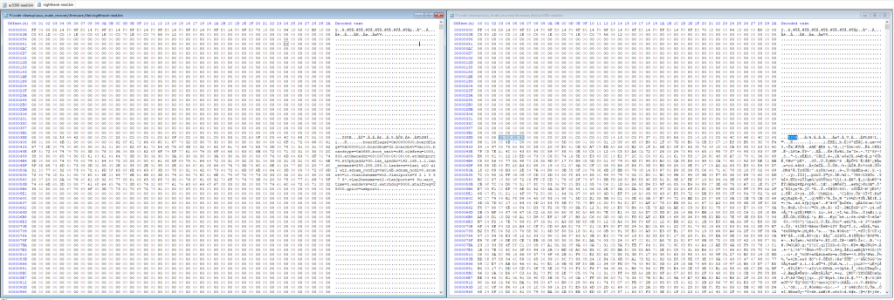
attached is a picture comparing the start of both NAND dumps ,
now it seems the nand layout is as follows
0x0-0x3f reset vector table maybe ?
0x3e0-0x3ff ZSIB - magic header for CPU to configure with
0x400-??? - FLSH - magic header for NVRAM config , defined in the source code with #define NVRAM_MAGIC 0x48534C46 /* 'FLSH' */, found the the file bcmnvram.h in merlin source codes. note the little indian cpu loading here
Now here where you will note the first real changes, the left image is the nighthawk and the right is the asus, you will note the asus has no text just garbled letters, well originally most thought it was encrypted , turn outs its not , it is LZMA compressed with a slight altered dictionary table ,
This is the nvram for the rt-ac5300 thats stored there , the tool to decompress it is found here , it does take some patching to compile and at some point i will upload my working source code and guide to my github,
"note, will post link to nvram soon" over char limit
Well now that we dumped NVRAM area and decompressed it we can assume this point of the NAND is good up to this point or the LZMA decompress would fail, something to note.
Now the section we just dumped is only the NVRAM and the CFE follows that ,
the entire cfe actually starts at 0x414 (hex search for 5D 00 00 01) and can be decompressed with this tool LZMA or LZMA_4K found here , this will decompress the routers cfe code, if you wish to dig deeper right now before i write up my own solution the see this chinese write up here , it also covers building the cfe and reverse engineering this ,
here is dump I extracted, it's the uncompressed cfe as loaded into ram, found here ,
So again, we have decompressed the data so again this section of NAND is good, well in this specific case,
if i run binwalk on the extracted nand i get this following
Next will extract the trx side of the firmware (magic code is HDR0 in firmware sources , source code is found here on github )
I will write up the next section soon.
darkspr1te
In this thread i will be covering NAND reading, ecc systems, CFE's , bootloaders in general , JTAG , software source code & compiling.
It wont be a easy read to do guide as it's a project in motion and I may incorrectly cover items initially.
So the short story is i have a few bcm47xx arm routers in a bin of electronics I collect and i figured i would give a crack at reverse engineering and possibly reviving these routers, documenting it along the way.
I am in now way a super coder, hacker or what ever just a hobbyist who likes a challenge and this policy has allowed me to recover quite a few devices in the past and come up with usable end-user solutions, and the documentation also allows others to learn and also transfer the methods to other or similar devices.
So onto the meat and potatoes of it.
My two subjects are one Asus rt-ac5300 and one netgear nighthawk x6,
Both contain the same main CPU a Broadcom BCM4709C0KFEBG dual-core @ 1.4 GHz
Both use the Spansion S3ML01G1 Nand device
both have full JTAG points and respond to ID_CODE requests
Now at the time these originally came across my desk two years ago there was no info on the JTAG side and even less about the CFE in use, how it works etc but thats changed a little and it's worth revisiting.
So far I have now removed both NANDS from the system dump via other means, I used a STM32 dev board,
found here VCCGND mini407
Once that was done i ported the NANDO firmware from the original stm32f103 chip to a stm32f407 based chip, found here for the nando original firmware and my port is here
and after some issues, head scratching , reaching out to experts (see that dialog here ) i finally have direct nand dumps (including spare area) to work with.
Those files can be found here , so far online i have not found copies of the ac5300 cfe,nvram table or even nand files so these may be the only copies online as most have given up or replaced the h/w so there is little desire to work to get them.
now out of the two units i will be digging into the ac5300 in more depth and use the nighthawk as example of changes between two providers and how that might possibly allows us to fix the ac5300
attached is a picture comparing the start of both NAND dumps ,
now it seems the nand layout is as follows
0x0-0x3f reset vector table maybe ?
0x3e0-0x3ff ZSIB - magic header for CPU to configure with
0x400-??? - FLSH - magic header for NVRAM config , defined in the source code with #define NVRAM_MAGIC 0x48534C46 /* 'FLSH' */, found the the file bcmnvram.h in merlin source codes. note the little indian cpu loading here
Now here where you will note the first real changes, the left image is the nighthawk and the right is the asus, you will note the asus has no text just garbled letters, well originally most thought it was encrypted , turn outs its not , it is LZMA compressed with a slight altered dictionary table ,
This is the nvram for the rt-ac5300 thats stored there , the tool to decompress it is found here , it does take some patching to compile and at some point i will upload my working source code and guide to my github,
"note, will post link to nvram soon" over char limit
Well now that we dumped NVRAM area and decompressed it we can assume this point of the NAND is good up to this point or the LZMA decompress would fail, something to note.
Now the section we just dumped is only the NVRAM and the CFE follows that ,
the entire cfe actually starts at 0x414 (hex search for 5D 00 00 01) and can be decompressed with this tool LZMA or LZMA_4K found here , this will decompress the routers cfe code, if you wish to dig deeper right now before i write up my own solution the see this chinese write up here , it also covers building the cfe and reverse engineering this ,
here is dump I extracted, it's the uncompressed cfe as loaded into ram, found here ,
So again, we have decompressed the data so again this section of NAND is good, well in this specific case,
if i run binwalk on the extracted nand i get this following
Code:
DECIMAL       HEXADECIMAL     DESCRIPTION
--------------------------------------------------------------------------------
2097152       0x200000        TRX firmware header, little endian, image size: 35651584 bytes, CRC32: 0x6C36F8DF, flags: 0x0, version: 1, header size: 28 bytes, loader offset: 0x1C, linux kernel offset: 0x1C2644, rootfs offset: 0x0
2097180       0x20001C        LZMA compressed data, properties: 0x5D, dictionary size: 65536 bytes, uncompressed size: 4486144 bytes
3941956       0x3C2644        Squashfs filesystem, little endian, version 4.0, compression:xz, size: 33801525 bytes, 3204 inodes, blocksize: 131072 bytes, created: 2021-08-06 22:24:14
37840154      0x241651A       xz compressed data
<snip repeats>
45809154      0x2BAFE02       xz compressed data
45836314      0x2BB681A       PNG image, 310 x 277, 8-bit/color RGBA, non-interlaced
45837210      0x2BB6B9A       Zlib compressed data, best compression
45923259      0x2BCBBBB       PNG image, 34 x 34, 8-bit/color RGBA, non-interlaced
45925007      0x2BCC28F       PNG image, 34 x 34, 8-bit/color RGBA, non-interlaced
45926562      0x2BCC8A2       PNG image, 34 x 34, 8-bit/color RGBA, non-interlaced
45927863      0x2BCCDB7       PNG image, 130 x 87, 8-bit/color RGBA, non-interlaced
45927941      0x2BCCE05       Zlib compressed data, best compression
45933139      0x2BCE253       PNG image, 97 x 71, 8-bit/color RGBA, non-interlaced
45933217      0x2BCE2A1       Zlib compressed data, best compression
45937344      0x2BCF2C0       PNG image, 97 x 71, 8-bit/color RGBA, non-interlaced
45937422      0x2BCF30E       Zlib compressed data, best compression
45940388      0x2BCFEA4       PNG image, 128 x 64, 8-bit/color RGBA, non-interlaced
45940466      0x2BCFEF2       Zlib compressed data, best compression
45955653      0x2BD3A45       PNG image, 130 x 87, 8-bit/color RGBA, non-interlaced
45955752      0x2BD3AA8       Zlib compressed data, best compression
45965257      0x2BD5FC9       xz compressed data
46021813      0x2BE3CB5       xz compressed data
46152749      0x2C03C2D       xz compressed data
46276821      0x2C220D5       xz compressed data
46339965      0x2C3177D       xz compressed data
46429682      0x2C475F2       PNG image, 66 x 66, 8-bit/color RGBA, non-interlaced
46429767      0x2C47647       Zlib compressed data, best compression
46432437      0x2C480B5       Zlib compressed data, best compression
46439299      0x2C49B83       PNG image, 90 x 270, 8-bit/color RGBA, non-interlaced
46439340      0x2C49BAC       Zlib compressed data, compressed
46453465      0x2C4D2D9       xz compressed data
46574265      0x2C6AAB9       xz compressed data
46668289      0x2C81A01       xz compressed data
46763137      0x2C98C81       xz compressed data
46858745      0x2CB01F9       xz compressed data
46891813      0x2CB8325       xz compressed data
46901241      0x2CBA7F9       xz compressed data
46954169      0x2CC76B9       GIF image data, version "89a", 580 x 344
47085241      0x2CE76B9       xz compressed data
<snip repeats>
49680373      0x2F60FF5       xz compressed data
73531392      0x4620000       JFFS2 filesystem, little endian
Next will extract the trx side of the firmware (magic code is HDR0 in firmware sources , source code is found here on github )
I will write up the next section soon.
darkspr1te
Attachments
Last edited: