The Cortex-A53 cores were designed for 28 nm from the beginning though, as a LITTLE companion core to the big A57. However, as we've seen, the A57 and also the A72 runs quite hot on the 28 nm node, but A53 never had an issue, as there are a ton of A53 chips out there. That was at least until companies started to increase the clock speed of the A53 cores way beyond what they were originally designed for.
However, as the article below mentions, the A53 was also designed to work with then future 20 and 16 nm nodes, which means Arm already prepared for designs on said nodes when they designed the cores.
Seeking answers? Join the AnandTech community: where nearly half-a-million members share solutions and discuss the latest tech.
www.anandtech.com
As mentioned above, it's not without risk to shrink a chip design to a new node and it's not entirely straightforward either and often requires new tools and sometimes even new licences or new IP blocks for it all to work. This is for example, why we've seen companies like AllWinner stick to their A7 and A53 cores for so long, whereas their competitors moved on to faster and sometimes better Arm cores.
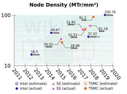
As also mentioned above, two similar nodes work very differently depending on the foundry used and even from the same foundry you have different node variants for power efficiency, performance etc. so just pulling a node figure out of ones hind side doesn't really mean much. Many companies have also become expert at optimising their chip designs for a specific node and have managed to eek out more performance and improve power efficiency without moving to a smaller node simply by optimising their chip designs.
On top of all that, the various IP blocks used together with the Arm core will affect on things like thermals, power draw and so on and here, it's really a lot of secret sauce from the router makers that simply can't be compared, as they all have different offload engines, DSPs and what not, that can actually draw a fair amount of power and as such produce a lot of extra thermals.
Taking this whole discussion to the next level, it also comes down to the router design itself, placement of components on the PCB and maybe most importantly, cooling of the power amplifiers, as those tiny chips often produce the most heat in a router and if they're on a shared heatsink with the SoC, they can affect the SoC temps quite significantly. In fact, one of the routers I was involved with, ended up being the first router with a heatpipe due to the power amplifiers and the dual core Cortex-A9 SoC we used running a tad too hot for the small housing that had been designed for the product. It solved the problem, but many router companies aren't willing to spend that extra cost, so they put in a fan or don't care if the router runs hot.
As such, this whole discussion is actually quite irrelevant.
As a data point, the BCM4912 in my GT-AX6000 runs at 57-58 degrees in an ambient temperature of around 24 degrees.