You are using an out of date browser. It may not display this or other websites correctly.
You should upgrade or use an alternative browser.
You should upgrade or use an alternative browser.
Linksys WRT1900AC First User Reports
- Thread starter thiggins
- Start date
@rmerliin - miniipnpd also supports NAT-PMP as well as uPNP, which is pretty handy
(NAT-PMP is part of the Bonjour/Rendevous/Avahi network stacks - Apple centric perhaps, but we're seeing other applications leverage Avahi as well)
uTorrent supports NAT-PMP, so I'm fairly sure there are a few other Win32 apps that does as well.
Somehow I thought that NAT-PMP support was fairly widespread. I take it the uPNP daemon used by Marvell (or Broadcom's own daemon) don't?
sm00thpapa
Very Senior Member
So would you replace your current router with it?
Sticking with this router. The console driver is the issue not the router. Microsoft releasing this console in 2011 with just a 2.4 GHz N card is a shame.
sfx2000
Part of the Furniture
Attachments

Last edited:

sfx2000
Part of the Furniture
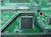
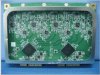
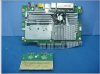
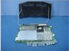
So, quick analysis here - nice stuff - I've designed a few devices, and Marvell was one of the vendors under consideration (due to NDA's and what not, can't really say, except that these were vertical carrier provided devices, and no, it's not with Arris or someone similar).
All in all, good clean design from a HW perspective, mostly a Marvell reference board, but this is a good thing - bit spendy compared to some others, but it's a beefy implementation for the most part. Chip count is higher here, as this is more of an enterprise/carrier grade oriented HW design - which explains the higher end-user cost, as the bill of material is going to be higher...
Getting into the HW from a Photo-Analysis - I haven't ripped my WRT1900ac review sample to confirm --- yet...
1) Armada XP, Marvell MV72830 - this is a dual core ARMv7 designed by Marvell - it's functionally equivalent to a Cortex-A9, but it's in-house - similar to what Qualcomm has done with Krait/Snapdragon and Apple with A6-Swift.
2) eSATA and USB2 - I suspect this is hosted on the Armada on the SERDES bus natively - they're not mux'ed, but do device detect based on electrical characteristics - clever...
3) GigE Switch is a Marvell 88E6172 "LinkStreet SOHO" - this is a 7-Port GE Switch w/ 5 integrated PHYs w/ 1GMII, RGMII, and EEE - I suspect this sits on one of the GigE ports on the Armada, the other GigE port I suspect hosts the WAN port for routing purposes - I could be wrong here, but I don't think so - 4 ports for back of the router, plus one upstream from the Armada XP - and the Armada XP has three GigE ports on it's own - so one for WAN, one to go the LinkStreet, and one for debug purposes - pretty standard for Marvell - getting terminal access into the WRT1900ac on the Linksys Firmware would be helpful for interface mapping...
4) USB3 - EtronTech EJ198H or similar, hard to tell as the photos are low Res - I suspect this sits on one of the PCIe lanes as a 1x - the Armada XP can either support one 4x or four 1x lanes
5) WiFi - Marvell Avastar 88W8864's - two of them, configured as single lane PCIe - integrated RF, these are 4*4 on the RF side, with three steams supported for SM - nice they're mounted on a daughterboard, so this opens up opportunities for alternate chipsets at some point
6) Flash Memory - hard to tell on the photos - but I suspect this is a Spansion 1Gb (128MB) NAND flash part, most likely S34ML01G2
7) RAM - Looks like Hynix parts here - likely in a 32 bit bus configuration, but I could be wrong here - these are BGA parts on 16 bits each - so it could also be 16 bit, but I'm ok with 32.
8) Since flash is NAND, the 256MB total memory space is actually not true - part of the flash is mirrored into RAM, as NAND cannot execute in place - considering that the compressed firmware image is approx 22MB, this gives us about 200MB of actual memory to work with - also note, as rMerlin has suggested, that the 128MB of flash - they keep a recovery image, so reduce flash by that amount - which gives us around 100MB or so outside of the firmware images - and then additional space for NVItems (settings), so it starts to get a bit tight for adding additional code...
I'll jump into SW in a bit... to summarize some of the interesting things there.
Last edited:
sfx2000
Part of the Furniture
uTorrent supports NAT-PMP, so I'm fairly sure there are a few other Win32 apps that does as well.
Somehow I thought that NAT-PMP support was fairly widespread. I take it the uPNP daemon used by Marvell (or Broadcom's own daemon) don't?
Interestingly enough - having picked thru Linksys' code - they integrate the BSP into their own code base, and that code base dates a long while back, pre-Cisco even - makes sense perhaps, as they need to support Broadcom and QC/Atheros, along with Marvell on the same mainline code...
Most apps that support NAT-PMP also support uPNP as a fallback - and uPNP is probably more universal, if less capable

subjectively speaking of course...
sfx
sfx2000
Part of the Furniture
your analysis is impressive, sfx, not that you need to hear it from me.
sorry, can't help it... I'm sure that there are errors in my assumptions, just looking at the HW, and having some design experience with HW/SW on these types of devices...
Thanks for the kind comment
")
sfx
sm00thpapa
Very Senior Member
My one issue is the speed of the 2.4 GHz band. Wired and on the 5GHz band I am getting my full 70 Mbps down load speed. On the 2.4 GHz band I am only getting anywhere between 10 and 30 Mbps. I am the only router on that channel. I have it set to N only, CH 6, 20MHz and WPA2-AES. I even tried the Mixed mode and it doesn't help.
chadster766
Very Senior Member
This is what I was able to get off the 2.4ghz.
----------------------------------------------------------
Intel Wireless N Adapter
Wireless N 2.4GHZ 20MHZ Channel Width
WLAN to LAN throughput: 56.178 Mbit/s
Wireless N 2.4GHZ Auto Channel Width
WLAN to LAN throughput: 97.700 Mbit/s
----------------------------------------------------------
----------------------------------------------------------
Intel Wireless N Adapter
Wireless N 2.4GHZ 20MHZ Channel Width
WLAN to LAN throughput: 56.178 Mbit/s
Wireless N 2.4GHZ Auto Channel Width
WLAN to LAN throughput: 97.700 Mbit/s
----------------------------------------------------------
This is what I was able to get off the 2.4ghz.
----------------------------------------------------------
Intel Wireless N Adapter
Wireless N 2.4GHZ 20MHZ Channel Width
WLAN to LAN throughput: 56.178 Mbit/s
Wireless N 2.4GHZ Auto Channel Width
WLAN to LAN throughput: 97.700 Mbit/s
----------------------------------------------------------
What's your ISP download speed on a wired LAN port?
Thanks.
chadster766
Very Senior Member
What's your ISP download speed on a wired LAN port?
Thanks.
7mbit/s down and 1mbit/s up from ISP.
My test is WLAN to LAN throughput. No WAN involved
")
7mbit/s down and 1mbit/s up from ISP.
My test is WLAN to LAN throughput. No WAN involved
Sorry, for some reason I misread WLAN as WAN, not sure why.
sm00thpapa
Very Senior Member
I had to cascade my WRT54G V4 to my WRT1900AC so my Xbox 360 upstairs can have internet. Hope a firmware upgrade corrects this issue.
sm00thpapa
Very Senior Member
All fixed ran the router in mixed mode on ch 1 and 6 which are clear. My cascaded router in now on ch 11 with my neighbor. Anyone know of a good AC1900 Adapter so I can test it with this router?
sm00thpapa
Very Senior Member
Moderate NAT again today on all of my Xbox 360's. 1 wired and 2 wireless. NAT is checked and so is UPNP. Never had this issue with my RT-N66U. This is getting very frustrating.
chadster766
Very Senior Member
Moderate NAT again today on all of my Xbox 360's. 1 wired and 2 wireless. NAT is checked and so is UPNP. Never had this issue with my RT-N66U. This is getting very frustrating.
This multiple xBox at one location issue is a problem with Asus (basically all) routers as well. I know this because a gaming friend of mine came to me for help that had a new Asus.
You are not going to believe the solution I gave him. It won't work for everyone because your ISP has to not be paying attention for it to work.
His internet is through a cable modem that was configured as a bridge. This modem could also be configured as a router and it has 4 Ethernet ports.
His previous router was a older Linksys E3000 which he still had left over after replacing it with the Asus.
I told him to plug both the Asus and E3000 WAN ports into the modem's Ethernet ports. Then I told him to make the SSID's different for the Asus and E3000.
After that I told him to power cycle the modem. Guess what each router got a Public IP Address!
So now when he is gaming with his brother one xBox connects to the Asus and one to the Linksys. Problem solved.
Then when he wants to transfer files or media they both connect to the same router.
Similar threads
- Replies
- 4
- Views
- 1K
- Replies
- 2
- Views
- 775
- Replies
- 17
- Views
- 1K
Latest threads
-
Release ASUS RT-AX68U Firmware version 3.0.0.4.388_24824 (2026/03/24)
- Started by fruitcornbread
- Replies: 0
-
Release ASUS RT-AX1800S V2 Firmware version 3.0.0.4.388_34015 (2026/03/24)
- Started by fruitcornbread
- Replies: 0
-
Mini-PCs running a desktop OS instead of retail NAS boxes
- Started by maxbraketorque
- Replies: 1
-
Release RT-AX88U Pro Firmware Version 3.0.0.6.102_37421 (2026/03/24)
- Started by wol-shiver
- Replies: 1
-
Support SNBForums w/ Amazon
If you'd like to support SNBForums, just use this link and buy anything on Amazon. Thanks!
Sign Up For SNBForums Daily Digest
Get an update of what's new every day delivered to your mailbox. Sign up here!